Important Progress in Electronics and Photonics Integration Made by SSE Prof. Zhaoyu Zhang’s Group
Recently, Prof. Zhaoyu Zhang`s group, from the School of Science and Engineering, demonstrated optically pumped photonic crystal lasers monolithically grown on silicon for the first time, which is an important progress in the field of electronics and photonics integration. Relevant results with title “Continuous-wave quantum dot photonic crystal lasers grown on on-axis Si (001)” were published in Nature Communications.
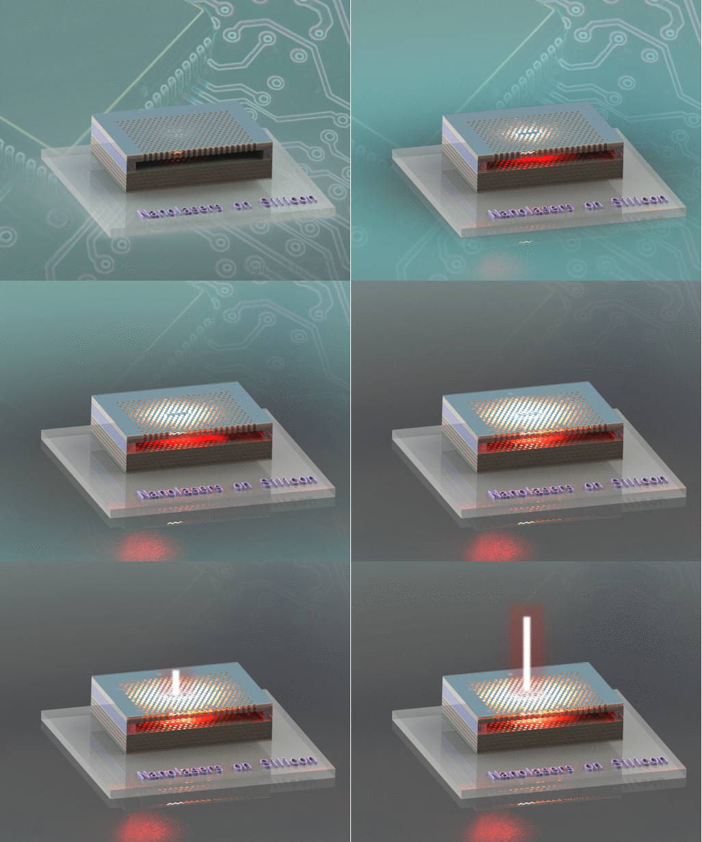
Figure 1. Schematic diagram of silicon-based quantum dots photonic crystal lasers chip.
In recent years, driven by the huge demand of optical communication and optical interconnection, silicon-based opto-electronic integration technology is developing vigorously. As one of most significant elements of silicon photonics. The modulation rate, integrated density and power consumption of lasers will directly limit the performance of silicon photonics. The silicon-based opto-electronic devices such as silicon waveguide, modulator and silicon detector have been well developed. However, owing to the fact that silicon is an indirect band gap semiconductor, which is not suitable for light-emitting devices. The Ш-V semiconductor materials (such as GaN, GaAs, InP, etc.) are direct band gap semiconductors, which are the most effective light-emitting materials for lasers. In the past 20 years, groups from CNRS in France, Intel and UCSB in the United States, NTT in Japan, and Hong Kong University of Science and Technology have put a great amount of effort in this field, to directly grow Ш-V materials on silicon. The goal is to integrate lasers on silicon with CMOS technology to achieve large-scale monolithic integration of silicon photonics, and finally to further improve the performance of optical communication devices with reduced cost. They have realized large-scale lasers on different silicon substrates, but have not yet demonstrated compact size nano lasers (photonic crystal lasers) on silicon substrates compatible with CMOS technology. In addition, the photonic crystal structure is considered to be an important element of future optical integration.
Prof. Zhaoyu Zhang`s group from the School of Science and Engineering and their collaborators designed the epitaxial structure of silicon-based quantum dot photonic crystal lasers and molecular-beam epitaxy (BME) was used to directly grow high-quality InAs quantum dots on silicon as the gain medium of the laser. Relying on the support from Shenzhen Key Lab of Semiconductor Lasers established in recent years, Prof. Zhaoyu Zhang`s group fabricated and tested the sub-wavelength scale photonic crystal lasers for the first time. The laser chips operate at room temperature under continuous-wave optical pumping. Single-mode lasing emission at 1310 nm optical communication band was achieved as shown in Figure 2.
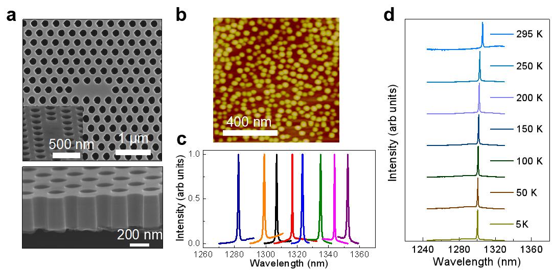
Figure 2. The device characteristics.
This is the another important research achievement made by Prof. Zhaoyu Zhang`s group in the field of silicon photonics (relevant research results were published in Optica in 2019). The first author of this Nature Communications paper is Mr. Taojie Zhou, a PhD candidate from the School of Science and Engineering. Dr. Mingchu Tang from University College London (UCL) is the co-first author. The co-corresponding authors of this paper include Prof. Zhaoyu Zhang from CUHKSZ, Prof. Huiyun Liu and Prof. Siming Chen from the UCL. Prof. Thierry Baron from the University Grenoble Alpes in France also contributes to this work.
Prof. Zhaoyu Zhang mentioned, “Our research work was mainly experimental research, without the support of different research institutes and laboratories, we could not push our research so far. Our work has been greatly supported by Prof. Xin Cheng and Dr. Xuexuan Qu from the Micro and Nanofabrication Facility of Southern University of Science and Technology in device preparation, Prof. Baoquan Sun from the Institute of Semiconductors, the Chinese Academy of Sciences and Prof. Chunlei Yang from Shenzhen Institute of Advanced Technology, the Chinese Academy of Sciences in device characterization.”
First author: Mr. Taojie Zhou

Mr. Taojie Zhou received his bachelor degree in 2016 from Boling class, School of Physics, Nankai University. Then he joined Prof. Zhaoyu Zhang`s group after graduation and is now engaged in the research of semiconductor micro- and nano-lasers. Some relevant research results are published in Nature communications, Optica, Optics Express, Applied Physics Letters, AIP Advanced, etc.
Prof. Zhaoyu Zhang

Prof. Zhaoyu Zhang received his Ph.D. degree from California Institute of Technology in 2007 in Electrical Engineering. From 2008 to 2011, he was a postdoctoral fellow in University of California, Berkeley, with a joint appointment at Lawrence Berkeley National Laboratory. From 2011 to 2015, he was an Associate Professor at Peking University and established a team of “Nano OptoElectronics Lab (NOEL)”. In 2015, he and his team moved to The Chinese University of Hong Kong, Shenzhen. In 2016, he was appointed the director of Shenzhen Key Laboratory of Semiconductor Lasers. His main achievements include the first demonstration of red-emission photonic crystal lasers, subwavelength-scale micro-lasers with physical size smaller than 1 micron, microfluidic microlasers based on dye materials, as well as the first demonstration of photonic crystal lasers directly grown on silicon substrates. He has published more than 20 referred papers on renowned journals including Nature Communications, Advanced Materials, Physics Review Letters, Optica, Photonics research, Optics Letters, Applied Physics Letters, etc.
The research of Prof. Zhang’s group (NOEL) focuses on applied nano-optics and nano-photonics. The technology is expected to be mature in 5-10 years, and the group’s mission is to train technical talents in the future optics and photonics industry. Currently, the group is mainly working on: 1. Micro laser devices and optoelectronic integration for future optical communication and face recognition; 2. Organic optoelectronic devices and integration for future display and lighting. The group has the capability of device fabrication and measurement, including ICP-RIE, thermal evaporation system, a femto-second laser, pico-second lasers, nano-second lasers, a streak camera, a cryo-stage, spectrometers, semiconductor parameter analyzers, an integrating sphere, etc.
Please check the group webpages for details.

